Takayuki Ohba Laboratory,
WOW Alliance Heterogeneous and Functional Integration Unit,
Institute of Integrated Research, Science Tokyo
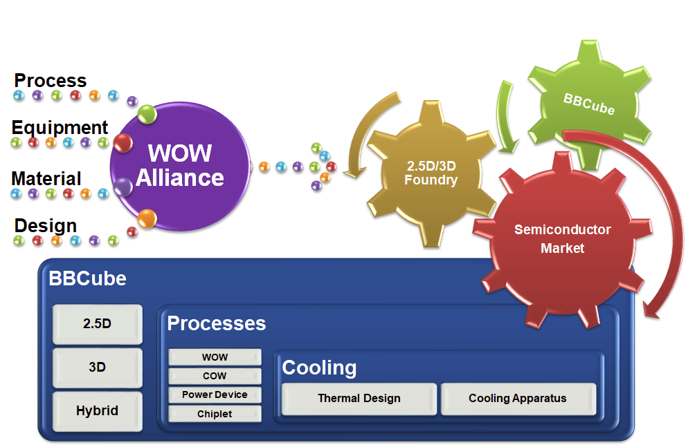
The WOW Alliance aims to address the physical limitations of planar scaling by enhancing volumetric integration density through wafer stacking. We have developed a breakthrough technology that enables the multilayer stacking of ultra-thin wafers—only 10 μm thick—while simultaneously forming Damascene interconnects. This bumpless stacking approach, known as BBCubeTM, is being transitioned toward practical deployment via a dedicated 300 mm pilot line for the semiconductor industry.
The WOW (Wafer-on-Wafer) and COW (Chip-on-Wafer) processes utilize 300 mm wafers that are fully compatible with conventional Front-End manufacturing, enabling seamless integration and significant cost reduction. In addition, COW technologies for chiplet applications also support bumpless Damascene wiring, allowing high-density 3D integration of heterogeneous functional devices. By integrating WOW and COW, BBCube 3D achieves up to a 1/1000 reduction in power consumption compared to conventional architectures.
To adapt flexibly to rapid technological evolution in semiconductors, the WOW Alliance collaborates with more than 40 private semiconductor companies through various R&D programs. As market needs shift toward system-level integration, the Alliance provides a comprehensive semiconductor platform encompassing circuit, power, and thermal design, along with supporting process, equipment, materials, analysis, and metrology.
Research Unit Leader Takayuki Ohba

Takayuki Ohba Profile
2013 Tokyo Institute of Technology, Professor
2004 The University of Tokyo, Professor
1984 Fujitsu Limited
National Chiao Tung University (NCTU Taiwan)
Visiting Professor
Ph.D received from Tohoku University in 1995
Tokyo Tech WOW Alliance
3-micronmeter Ultra-Thinnig 300mm SDRAM


Three-Dimensional Integration Process Technology
We will use the ultra-thinning technology and the vertical interconnect technology possessed by the WOW Alliance to integrate semiconductors three-dimensionally and create a next-generation semiconductor that is higher in performance and lower in power consumption. Furthermore, this work will accelerate the ultra-miniaturization of not only large-scale computing devices such as servers, but various devices equipped with semiconductors to 1/1000th of their current size.
Three-Dimensional Integration Design and Architecture
We propose 3DI architecture and design technology that make use of BBCube's excellent electrical and thermal characteristics such as low capacitance, low inductance, and low thermal resistance, and accelerate high performance, low power consumption, and miniaturization in a wide range of devices, from HPC/AI to sensor-integrated edge devices.
Three-Dimensional Integration Cooling Technology
By combining ultra-small cooling devices with three-dimensional stacked semiconductors, our work will allow for simplification of cooling technology and application to the miniaturization of IoT and mobile devices.
Wide Band Gap Semiconductor
Aiming to promote green innovation using wide band gap power devices, from the perspective of material science to system device application.
Specifically, focusing on low-cost epitaxial technology and thermal management technology, the goal is to develop them into 3D-integration technology.